The idea: a memory made of two switches and two inverters
A latch built from logic gates (NOT, AND and NOR) works, but every gate costs 4 to 6 transistors. Chip designers build the same latch from transmission gates and inverters, which needs only 12 transistors. Two inverters in a loop keep each other's value forever. Two switches, worked by the clock, decide whether that loop is closed (the latch holds its bit) or whether new data from D is let in instead.
On the canvas, wires at 1 are dark blue and wires at 0 grey. A transistor channel that conducts is green; an open one is white. The small chips show the value on each node. Press Toggle CLK and Toggle D to drive the inputs, or pick a demo. Each press is one column of the timing diagram.
The transmission gate
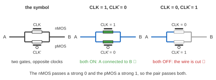
An nMOS transistor conducts when its gate is 1, a pMOS when its gate is 0 (see The Transistor as a Switch). An nMOS alone passes a 0 well but a 1 badly: its output stops one threshold voltage below VDD. A pMOS is the other way round. A transmission gate puts both in parallel, with CLK on the nMOS gate and CLK̄ (the inverted clock) on the pMOS gate. The two are then always both ON or both OFF. When ON, whichever value comes in, one of the two passes it at full strength. CLK̄ is made by one clock inverter (2 transistors) shared by the whole circuit.
The 12-transistor D latch
The latch has three inverters and two transmission gates:
- I1 inverts D. It buffers the input, so the outside world never drives the inner node directly.
- T1 is ON when CLK = 1 and connects D̄ to the inner node X.
- I2 inverts X and drives the output Q. Two inversions, so Q = D.
- I3 inverts Q back to Q̄, and T2 (ON when CLK = 0) connects Q̄ to X. Together, I2 and I3 form a loop.
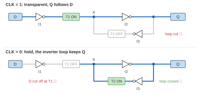
While CLK = 1, T1 is ON and T2 is OFF. Any change of D runs through I1, T1 and I2 to Q, so Q follows D: the latch is transparent (Demo: latch transparent). When CLK falls to 0, T1 cuts D off and T2 closes the loop. Q̄ already has the same value as X, so nothing changes at that moment. From now on the two inverters drive each other and hold the bit as long as the power is on. A new D only reaches T1 and stops there (Demo: latch holds).
Every node always has exactly one driver. Either T1 drives X (and T2 is open) or T2 does (and T1 is open). The two never fight, so no current flows from VDD to ground except while a node switches.
Counting transistors
| circuit | built from | transistors |
|---|---|---|
| D latch from gates (Sequential Logic) | NOT (2) + 2 AND (6 each) + 2 NOR (4 each) | 22 |
| D latch from transmission gates | 3 inverters + 2 TGs + clock inverter | 12 |
| flip-flop from gates | two gate latches + clock inverter | 44 |
| flip-flop from transmission gates | 5 inverters + 4 TGs + clock inverter | 20 |
A chip holds millions of flip-flops, so halving their size matters for area, power and speed. The price is that this latch needs both clock polarities, and it relies on a careful circuit design rather than on gates that a synthesis tool can rearrange freely.
The master–slave D flip-flop
A flip-flop is two latches in a row on opposite clocks. The master (I1, T1, I2 and its loop I3, T2) is transparent while CLK = 0. Its output M follows D. The slave (T3, I4, I5 and its loop through T4) is transparent while CLK = 1. Because the slave gets M without an input inverter, the flip-flop needs only 5 inverters: 20 transistors with the shared clock inverter.
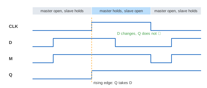
- CLK = 0: T1 ON, the master follows D. T3 OFF, so the slave does not see M; T4 ON, so the slave holds Q.
- CLK rises: T1 turns OFF and T2 ON, so the master freezes the last D. At the same time T3 turns ON and copies M through I4 and I5 to Q.
- CLK = 1: D can change as it likes; it stops at T1. Q does not move.
- CLK falls: the slave closes its loop and keeps Q; the master starts following D again.
So Q changes only at the rising edge, and then takes the value D had just before it (Demo: flip-flop edge). There is never a moment when both latches are open, as long as CLK and CLK̄ switch together.
Dynamic latches
Drop I3 and T2 and the latch still works for a while. When T1 turns OFF, node X is cut off from every driver, but the gate of I2 behind it is a small capacitor. The charge on it keeps X at its value, so Q stays put. This dynamic latch needs only an input inverter, one transmission gate and an output inverter. The charge slowly leaks away through the OFF transistors, though, so the value is lost if the clock stops for longer than a few microseconds to milliseconds. The feedback loop of the static latch on this page refreshes X all the time, so it keeps its bit while the clock is stopped. DRAM uses the same idea as the dynamic latch and must be refreshed for the same reason.
What the page leaves out
- Time. Every stage switches at once, one step after the other. Real inverters and transmission gates take tens of picoseconds, which gives the flip-flop its setup time, hold time and clock-to-Q delay (see Sequential Logic).
- Clock skew. If CLK̄ lags behind CLK, T1 and T3 can be on together for a moment and D races through both latches. Real designs size the clock inverter and the gates carefully to avoid it.
- Voltages and sizing. Values are just 0 and 1. The feedback inverter of a real latch is made weak, so that the input path can overpower it, and many designs put a small gate on the feedback path instead of a full transmission gate.
- Reset, enable and scan. Flip-flops in real chips often add a reset input, an enable and a scan input for testing.
References
Harris and Harris, Digital Design and Computer Architecture, section 3.2.7: transistor-level latch and flip-flop designs, and section 1.7 on CMOS transistors and transmission gates
Weste and Harris, CMOS VLSI Design, chapter 10 (sequential circuit design): static and dynamic latches, conventional CMOS flip-flops