The idea: code that describes hardware
A hardware description language (HDL) such as Verilog or SystemVerilog looks like a programming language, but it does not run line after line. It describes a circuit. A synthesizer (Vivado, Quartus, Yosys, Design Compiler) reads the code and turns each construct into gates, multiplexers and registers. Then all of that hardware works at the same time.
So the useful skill is to read a line of HDL and see the hardware it will make. The page shows a short snippet on the left and the circuit on the right. Synthesize lights up one line at a time, flies its code over, and draws the hardware it becomes in the same orange. Simulate then applies a row of inputs (or one clock edge) and colours each wire: green for 1, grey for 0.
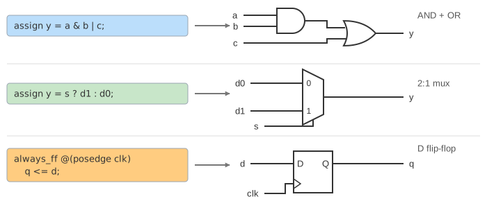
assign: gates and muxes
An assign statement is continuous: the left side always equals the right side. That is exactly what combinational logic does, so the synthesizer builds gates. In assign y = a & b | c; the & binds tighter than |, so it is (a & b) | c: an AND gate feeding an OR gate. One line, two gates. (Demo: an assign becomes gates.)
The conditional operator s ? d1 : d0 picks one of two values, which is a 2:1 multiplexer with s on its select input. With 4-bit d0 and d1 the tool simply builds four of them, one per bit. (Demo: ?: becomes a mux.)
| Code | Hardware |
|---|---|
&, |, ^, ~ | AND, OR, XOR gates, inverters |
s ? d1 : d0 | 2:1 multiplexer |
a + b, a == b | an adder, a comparator (built from gates) |
always_comb case | a decoder or a wide mux |
always_ff @(posedge clk) | flip-flops |
always_ff: flip-flops, reset and enable
always_ff @(posedge clk) q <= d; says: at every rising edge of clk, copy d into q, and hold it until the next edge. That is a D flip-flop. Every signal assigned inside an always_ff block becomes a flip-flop (or a bank of them for a bus).
Two common variants change the hardware a little:
- Asynchronous reset:
@(posedge clk, posedge reset)withif (reset) q <= 0;first. The reset goes to the flip-flop's own reset pin, so it clearsqat once, without waiting for the clock. A synchronous reset (onlyposedge clkin the list) would instead be an AND gate in front of D. - Enable:
else if (en) q <= d;. Whenenis 0 nothing is assigned, and inalways_ffthat simply means "keep the value". The hardware is a mux in front of D that feedsqback, so the flip-flop reloads its own value.
In Demo: flip-flop with reset and enable, row 1 has reset = 1 and q is 0 before the edge; row 2 has en = 0 and q stays 0 although d = 1; row 3 loads 1; row 4 keeps 1 although d = 0; row 5 loads 0.
always_comb and case: a decoder
always_comb marks a block of combinational logic: its outputs are recomputed whenever an input changes. A case that sets one output bit for each value of a is a decoder. Each case item becomes one AND gate that is 1 for exactly one value of a (a minterm); a bubble on an AND input means that bit must be 0. (Demo: case becomes a decoder.) A case that picks one of several data inputs would become a wide multiplexer instead.
The latch you did not mean to create
In combinational logic every output must have a value for every input. Look at this block:
always_comb
  if (en) q = d;      // and when en = 0?
When en is 0 no line assigns q. The language says q then keeps its old value. Gates cannot remember anything, so the synthesizer adds a latch, a storage element that is open (transparent) while en = 1 and holds while en = 0, and prints a warning such as "latch inferred for q". The code looked like logic; the hardware has memory.
In the demo, row 3 shows the bug: en = 0 and d = 0, but q is still 1. Adding else q = 1'b0;, or a default assignment q = 1'b0; before the if, gives q a value on every path, and the same idea becomes one AND gate: q = en & d. (Demo: the latch you did not mean, and the fix.)
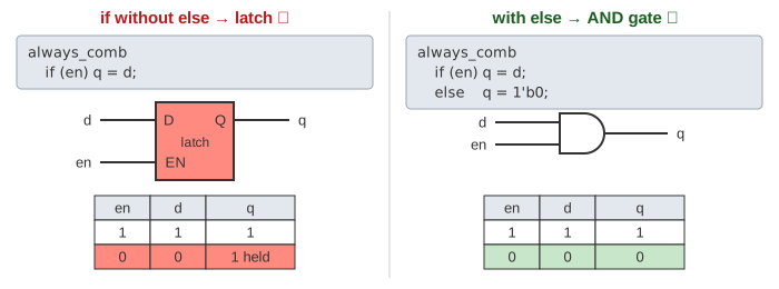
Latches are not wrong in themselves, but an unplanned one breaks timing analysis and makes the circuit depend on how long en is high. always_comb helps: many tools warn or fail when an always_comb block infers a latch. If you really want one, write always_latch.
Blocking (=) vs nonblocking (<=)
Inside an always block there are two kinds of assignment:
- Nonblocking
<=: all right sides are read first, with the values from before the edge, and all left sides change together at the end. This matches flip-flops, which all sample at the same clock edge. - Blocking
=: each line takes effect immediately, so the next line already sees the new value, like a program.
Take a three-stage shift register. With <=, q2 <= q1 reads the old q1, so each value moves one stage per edge: three flip-flops in a chain. With =, q1 = d runs first, then q2 = q1 reads the new q1, which is already d, and q3 too. All three equal d, so the tool builds one flip-flop and wires all three outputs to it. (Demo: <= vs = in a shift register.)
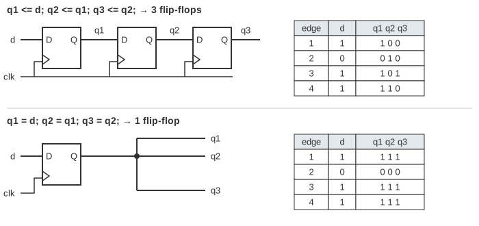
| Edge | d | with <= (q1 q2 q3) | with = (q1 q2 q3) |
|---|---|---|---|
| 1 | 1 | 1 0 0 | 1 1 1 |
| 2 | 0 | 0 1 0 | 0 0 0 |
| 3 | 1 | 1 0 1 | 1 1 1 |
| 4 | 1 | 1 1 0 | 1 1 1 |
Rules of thumb
- Clocked logic:
always_ff @(posedge clk)and only<=. - Combinational logic:
assign, oralways_combwith=, and give every output a value on every path (anelse, adefault, or a default assignment at the top). - Assign each signal in only one
alwaysblock orassign. - Read the synthesis report: count the flip-flops and look for "latch" warnings. If the numbers surprise you, the code does not say what you meant.
See also Combinational Logic for these gates and muxes switching with real delays, Sequential Logic for how a latch and a flip-flop are built from gates, Finite State Machines for the state register plus next-state logic that an HDL FSM becomes, and Memory Arrays for the lookup tables an FPGA uses to hold this logic.
What the page leaves out
Real synthesis optimizes the logic (Boolean minimization, sharing, retiming) and maps it to a cell library or to FPGA lookup tables and flip-flops, so the netlist rarely looks as tidy as these drawings. Buses, parameters, generate loops, arithmetic operators, synchronous reset, simulation-only code (initial, delays like #5), X values and timing constraints are left out. The simulator here applies inputs one row at a time with no gate delays.
References
Sarah L. Harris and David Harris, Digital Design and Computer Architecture, chapter 4: Hardware Description Languages (combinational logic, sequential logic, blocking and nonblocking assignments, latches)
IEEE 1800-2017: SystemVerilog unified hardware design, specification and verification language